X-ray inspection systems are widely used in many industry sectors such as:
Non-destructive testing of semiconductor devices and PCB allow investigation of hidden areas such as the wire bonding and the quality of solder reflow of components such as BGAs.
During X-ray inspection, high magnification images of micron level should be displayed. This leads the electronic components to be highly irradiated.
Too high a dose may damage some components.
For the manufacturer and integrator of PCB, the danger of the radiation dose during X-ray inspection could be the physical damage caused by high dose. An example is the surface damage of semiconductors
The other potential concern is for subtler failure such as bit flips, loss of program, leakage, etc., with probability of failure being difficult to assess and with physical damage remaining invisible or difficult to detect.
Components of concern are semiconductor devices such as Flash memory, DRAM, microprocessors… with potential failure starting from 20 Gy (Si)
Therefore, it is important to monitor the dose being received by these items during the X-ray inspection process and make sure that dose thresholds are not exceeded. Those thresholds should consider the dose integrated during the product lifetime.
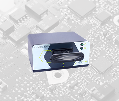
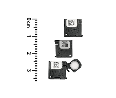
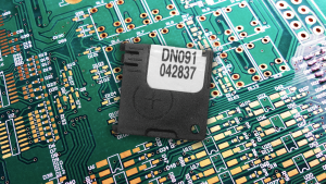
LANDAUER proposes microSTARii dose monitoring system which allows to monitor the dose received by the PCB. The small size of the nanoDot and robustness allows easy installation at the desired location on the PCB.